Deposition Process Equipment
Deposition process equipment forms nanoscale thin film to make circuits on wafers.
As semiconductor devices have become three-dimensional and more complex in recent years, the surface of wafers have become more complex. This in turn has increased demand for highly difficult deposition.
Our deposition process equipment supports LP-CVD*1, oxidation, annealing (low and high temperature), diffusion, and ALD*2 technologies, and has earned high acclaim from semiconductor device manufacturers worldwide.
*1. Low Pressure Chemical Vapor Deposition
*2. We refer to a technique for thin-film deposition at an atomic layer level involving a process of cyclical supply of multiple gases as “ALD”.
-
 Mini Batch Deposition Equipment
Advanced TSURUGI Plus-Ⅲ 剱
Process Applications
-
Thin film deposition
Advanced TSURUGI Plus-Ⅲ 剱 is the top model in our deposition process equipment line. This thermal processing platform is capable of both highly difficult deposition and high productivity on next-generation devices that have increasingly precise and minute structures. Thanks to greatly increasing the surface area that needs for film forming and adopting new technology that achieves highly difficult deposition on 3D stacked devices with increasingly complex structures, the platform can provide high-quality processing.
-
-
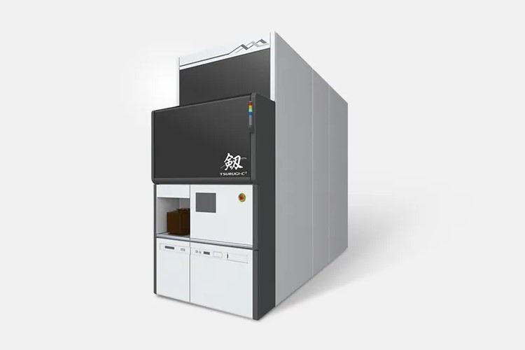
Mini Batch Deposition Equipment
Advanced TSURUGI 剱
Process Applications
-
Thin film deposition
Advanced TSURUGI 剱 is a thermal processing platform that is capable of both highly difficult deposition and high productivity on next-generation devices that have increasingly minute and complex structures. It can provide high-quality processing by using a new reactor that achieves highly difficult deposition on 3D stacked devices.
-
-
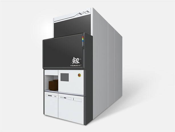
 Mini Batch Deposition Equipment
TSURUGI-C²® 剱®
Process Applications
-
Thin film deposition
TSURUGI-C²® 剱® is a thermal processing platform that is capable of both highly difficult deposition and high productivity on next-generation devices. It is equipped with a wafer reactor and other deposition technologies to enable high-quality processing.
-
-
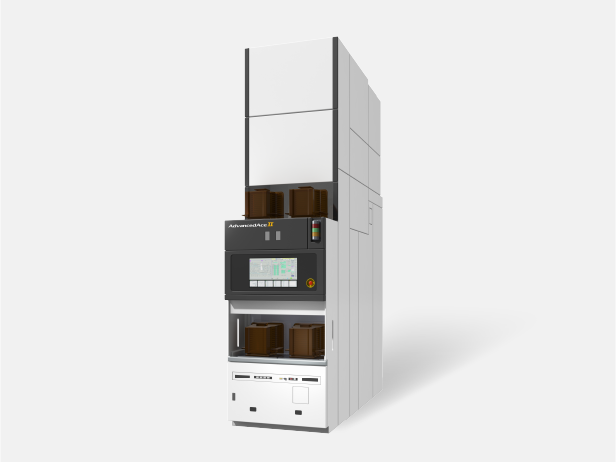 Large Batch Deposition Equipment
AdvancedAce®-II
Process Applications
-
Thin film deposition
-
CVD/oxide film deposition
AdvancedAce®-Ⅱ is a KOKUSAI ELECTRIC’s latest platform for batch thermal processing of 300mm wafers.
AdvancedAce®-Ⅱ offers high throughput by utilizing advanced technologies in such areas as temperature control, wafer handling automation, reactor purging. -
-
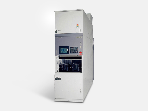
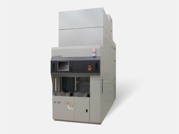
 Large Batch Deposition Equipment
QUIXACE®-II
Process Applications
-
Thin film deposition
-
CVD/oxide film deposition
QUIXACEI®-Ⅱ is a KOKUSAI ELECTRIC’s latest platform for batch thermal processing of 300mm wafers. QUIXACEI®-Ⅱ offers high throughput by utilizing advanced technologies in such areas as temperature control, wafer handling automation, reactor purging.
-
-
 Large Batch Deposition Equipment
VERTRON® Revolution
Process Applications
-
Thin film deposition
-
CVD/oxide film deposition
“VERTRON® Revolution” is the latest product in our proven VERTRON® series of 200-mm batch thermal processing systems. Customers can choose from a variety of models to suit their needs — from high-mix low-volume production to mass production. It is also compatible with 150-mm or smaller wafers.
-
-
 Large Batch EPI Deposition Equipment
QUIXACE®-LV
Process Applications
-
Thin film deposition
QUIXACEI®-LV is a KOKUSAI ELECTRIC’s latest platform for batch thermal processing of 300mm wafers.
QUIXACEI®-LV offers high throughput by utilizing advanced technologies in such areas as temperature control, wafer handling automation, reactor purging.
The vacuum load-lock structure of the wafer loading area greatly reduces native oxide film and contamination, making higher quality deposition possible. -


Treatment (film property improvement) Process Equipment
Treatment process equipment improves film properties by applying plasma and heat on thin film to remove impurities from film and stabilize particles.
As semiconductor devices have become more minute and complex in recent years, demand has grown for treatment technology that can improve film properties in low-temperature environments.
Our treatment equipment supports nitridation, oxidation, curing, and annealing, and has earned high acclaim from semiconductor device manufacturers worldwide.
-
 Single Wafer Treatment Equipment
MARORA®
Process Applications
-
Plasma nitridation(Nitridation of dielectric film)
-
Plasma oxidation(Forming thin oxidation film/Selective oxidation/Anisotropic oxidation)
MARORA® is a suitable tool to provide gate dielectric film for next generation DRAM, logic or flash memory.
With our original plasma generation method (MMT*), MARORA® generates a plasma with low electron temperature (approx. 1eV) efficiently and realizes plasma damage free process. -
-
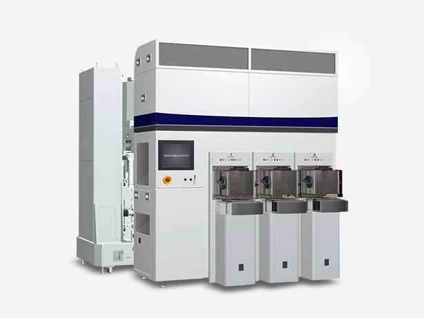
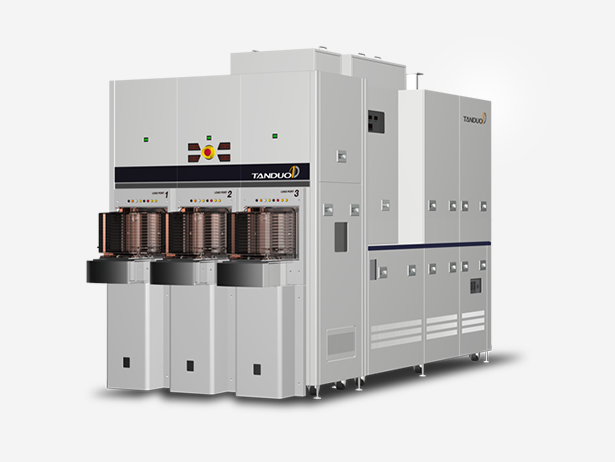 Single Wafer Treatment Equipment
TANDUO®
Process Applications
-
Low temp Annealing
-
Curing
TANDUO® provides an optimized system for the process such as curing, annealing and degassing by module selection.
We have achieved great productivity and low particle process environment with our original high-speed wafer transfer system. -
-
Large Batch Treatment Equipment
AdvancedAce®-II
Process Applications
-
Oxidation
-
Diffusion
-
Annealing (low/high temp.)
AdvancedAce®-Ⅱ is a KOKUSAI ELECTRIC’s latest platform for batch thermal processing of 300mm wafers.
AdvancedAce®-Ⅱ offers high throughput by utilizing advanced technologies in such areas as temperature control, wafer handling automation, reactor purging. -
-
Large Batch Treatment Equipment
QUIXACE®-II
Process Applications
-
Oxidation
-
Diffusion
-
Annealing (low/high temp.)
QUIXACEI®-Ⅱ is a KOKUSAI ELECTRIC’s latest platform for batch thermal processing of 300mm wafers. QUIXACEI®-Ⅱ offers high throughput by utilizing advanced technologies in such areas as temperature control, wafer handling automation, reactor purging.
-
-
Large Batch Treatment Equipment
VERTRON® Revolution
Process Applications
-
Oxidation
-
Diffusion
-
Annealing (low, high, and ultra-high temperatures)
“VERTRON® Revolution” is the latest product in our proven VERTRON® series of 200-mm batch thermal processing systems. Customers can choose from a variety of models to suit their needs — from high-mix low-volume production to mass production. It is also compatible with 150-mm or smaller wafers.
-

