Semiconductors
What is a semiconductor?
Substances are either a “conductor” that conducts electricity like metals or an “insulator” that does not conduct electricity like glass or rubber. Substances with properties that fall between those two are called a “semiconductor.” Devices with semiconductors like transistors, diodes, and integrated circuits are called “semiconductor devices,” which are often abbreviated as “semiconductor.”
A semiconductor device can flexibly control the direction and amount of electrical current by utilizing the properties of a semiconductor, that of changing its electrical conductivity under certain conditions.

A semiconductor device is made of multiple layers of electronic circuits. Thin metal film is placed on a substrate called a wafer, which is then processed to create an electronic circuit. By repeating this process until there are many layers of circuits, you create a semiconductor device. Semiconductor devices have functions such as information storage and arithmetic processing, and play a key role as the brains of electronic devices.
Adding layers of film on a wafer and increasing the level of integration enhances the performance of a semiconductor device, so advancements in nanoscale processing technology for semiconductor devices are being made worldwide.
Semiconductor devices are an essential part of our lives
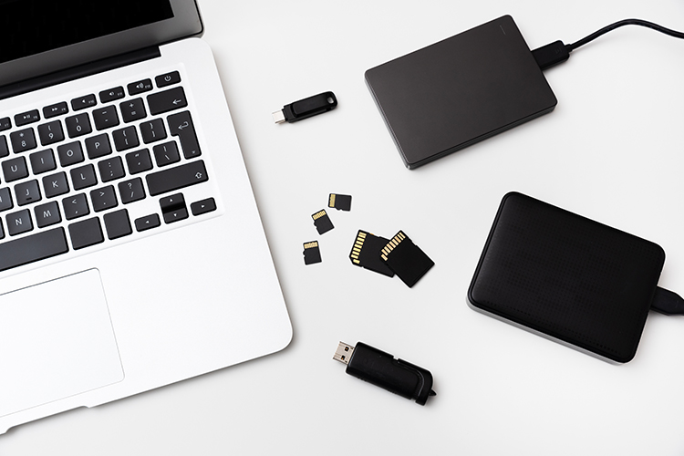
Semiconductor devices are used in a wide variety of places — everything from consumer goods like appliances, smartphones, computers, and cars to things that are essential for society such as trains, airplanes, and data centers. The more advanced features a product has, the wider variety of semiconductor devices it requires. For example, many of the parts that make up a computer — CPU, DRAM, and NAND flash memory — are semiconductor devices.
- CPU (Central Processing Unit)
-
The most important device in a computer. It controls other devices and circuits, performs arithmetic operations on data, etc.
- DRAM (Dynamic Random Access Memory)
-
A type of semiconductor memory. It is considered volatile memory, which means it stores information only when electricity is being supplied.
- NAND ("Not AND" logical operator)
-
A type of semiconductor memory. It is considered non-volatile memory, which means it stores information even when electricity is not being supplied.
Structure of the Semiconductor Industry
Size of the electronics and semiconductor manufacturing equipment market
How big is the semiconductor market?
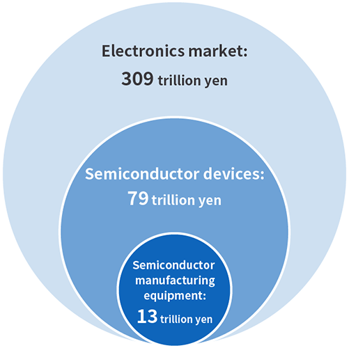
In 2022 the electronics market was 309 trillion yen, the market for semiconductor devices that are used in a variety of places was 79 trillion yen, and the market for semiconductor manufacturing equipment that is essential for making semiconductors was 13 trillion yen.
- Note:
-
30% of the world’s semiconductor manufacturing equipment is made in Japan (based on research conducted by KOKUSAI ELECTRIC).
- Source:
-
Gartner®, “Forecast: Semiconductor Capital Spending, Wafer Fab Equipment and Capacity, Worldwide, 4Q22 Update” Bob Johnson et al., 22 December 2022 (Exchange Rates per U.S. Dollar -Yen 132.82). From 2022 Revenue, Electronics market = Electronic Equipment Production, Semiconductor device market = Semiconductor Revenue, Semiconductor manufacturing equipment market = Total Wafer Fab Equipment. GARTNER is a trademark and service marks of Gartner, Inc. and/or its affiliates and are used herein with permission.
Calculations performed by KOKUSAI ELECTRIC.
- Note:
-
Charts/graphics created by KOKUSAI ELECTRIC based on Gartner research.
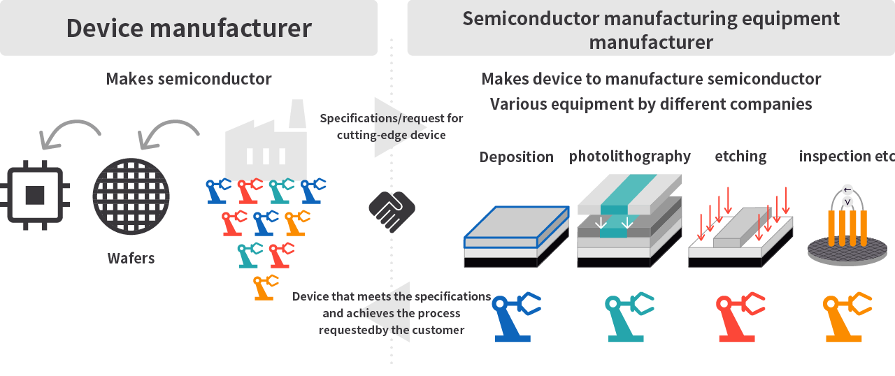
The device manufacturer that makes semiconductor devices tells the semiconductor manufacturing equipment manufacturer the specifications needed to make the semiconductor device. Then the semiconductor manufacturing equipment manufacturer develops equipment that meets those specifications, and sells it to the device manufacturer.
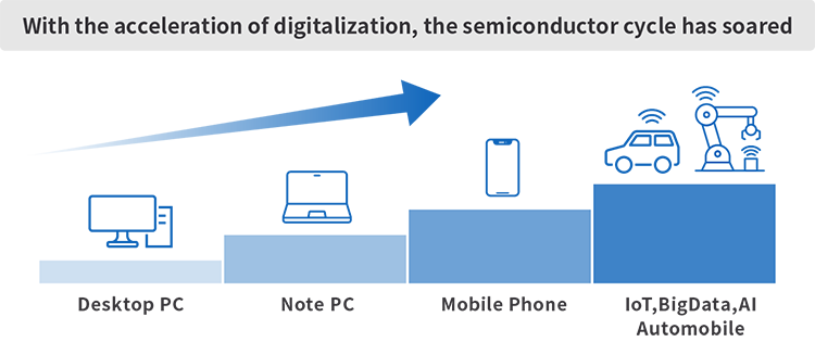
With the shift in demand from traditional consumer devices like mobile phones and computers to high-growth industry technologies such as data centers, 5G, and AI, the semiconductor device market is experiencing an expansion.
Semiconductor device demand continues to grow dramatically, and the market is expected to keep expanding over the long term.
In order to produce a large number of advanced semiconductor devices to meet the growing demand, semiconductor manufacturing equipment that balances highly difficult deposition with high productivity is needed.
Semiconductor Device Manufacturing Process
Manufacturing process and the role of the Group
There are two processes in the manufacturing of semiconductor devices. The front-end process consists of forming several layers of thin film on the surface of a wafer and designing electronic circuits. The back-end process consists of cutting out semiconductor chips from wafers, and packaging, assembly, and inspection.
Front-end Process
The semiconductor device front-end process consists of several stages: “deposition” in which thin film needed for creating electronic circuits is formed, “treatment (Film Property Improvement) ” for improving film properties with heat and plasma after deposition, “photolithography” to transfer circuit patterns designed in deposition, “etching” in which film is removed in line with patterning, “cleaning” in which the wafers are cleaned in between each stage, and “inspection” between each stage.
Circuits are layered by repeating these stages up to several 100 times on wafers.
The Group operates businesses that center on the front-end process stages of deposition and treatment (Film Property Improvement) . Combining both of these in a broad sense, the deposition stage plays an important role in forming circuits on wafers, so providing advanced technology and highly reliable products is essential for equipment. Our batch deposition and single wafer treatment systems — our flagship products — have earned high acclaim from semiconductor device manufacturers worldwide and boast among the highest share in the world.
- Batch deposition system
-
Equipment capable of deposition on multiple wafers at once.
- Single wafer treatment system
-
Equipment that can treat one wafer at a time.

Back-end Process
The back-end process consists of cutting out semiconductor chips from wafers, mounting chips on frames, connecting wires, packaging, and inspecting. Wafers have over 100 integrated circuits, so each one is cut out and assembled into products. Fabricating wafers after the front-end process requires high yield.
